Researchers have discovered a crucial recipe for improving the characteristics of graphene devices for use as photodetectors in the next generation of pholtovoltaic devices for telecommunications and energy harvesting.
Researchers have discovered a crucial recipe for improving the characteristics of graphene devices for use as photodetectors in the next generation of pholtovoltaic devices for telecommunications and energy harvesting.
The combination of graphene's unique optical and electronic properties with plasmonic nanostructures can be fully exploited, in a variety of useful devices, such as solar cells and photodetectors.
Andrea Ferrari
The findings are reported in the journal Nature Communications, and were made by a team from the Universities of Cambridge and Manchester which includes the Nobel Prize-winning scientists Professors Andre Geim and Kostya Novoselov.
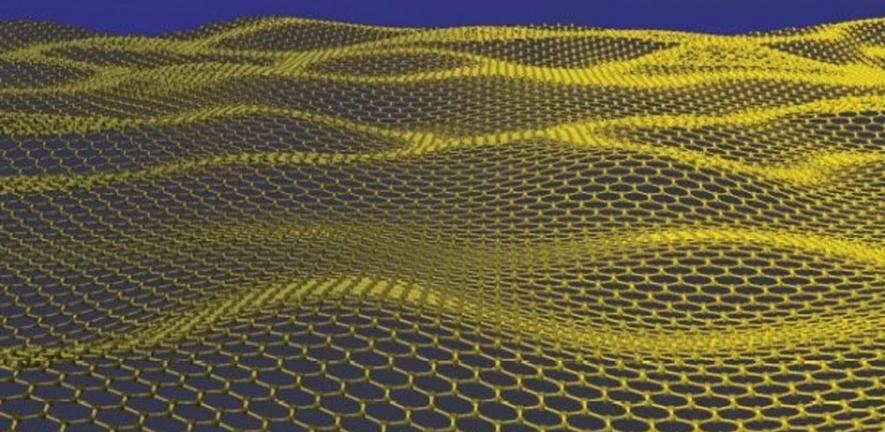
Graphene is a one-atom-thick sheet of carbon atoms arranged in a honeycomb lattice. It is a highly strong and extremely versatile substance and researchers believe that its potential applications are so numerous it could revolutionise fields such as electronics, information processing and energy storage.
In the new research, the team combined graphene with metallic nanostructures, leading to a twenty-fold enhancement in the harvesting of light to create energy. This paves the way for future advances in high-speed internet development and other communications.
Previous studies had already shown how graphene can be used to create an elementary solar cell. If two closely-spaced metallic wires are put on top of graphene and light is shone on the structure, it generates an electric voltage.
The major stumbling block towards practical applications for these otherwise very promising devices has so far been their low efficiency, however. The problem is that graphene – the thinnest material in the world – absorbs little light (approximately just 3%), while the rest goes through it without contributing to electrical power.
The Cambridge and Manchester team solved the problems by combining graphene with tiny metallic structures which are arranged on top of it. These so-called plasmonic nanostructures have dramatically enhanced the optical electric field felt by graphene and effectively concentrated light within the one-atom-thick carbon layer.
By using the plasmonic enhancement, the light-harvesting performance of graphene was boosted 20 times over, without sacrificing any of its speed. In future, the efficiency of graphene in this regard will be improved even further.
Professor Andrea Ferrari, from the Cambridge Engineering Department, who led the Cambridge effort in the collaboration, said: “So far, the main focus of graphene research has been on fundamental physics and electronic devices.”
“These results show its great potential in the fields of photonics and optoelectronics, where the combination of its unique optical and electronic properties with plasmonic nanostructures can be fully exploited, even in the absence of a bandgap, in a variety of useful devices, such as solar cells and photodetectors.”
Professor Novoselov, from the Manchester team, added: “The technology of graphene production matures day by day, which has an immediate impact both on the type of exciting physics which we find in this material, and on the feasibility and the range of possible applications.”
“Many leading electronics companies consider graphene for the next generation of devices. This work certainly boosts graphene’s chances even further.”
The paper, Strong Plasmonic Enhancement of Photovoltage in Graphene, by T. J. Echtermeyer, L. Britnell, P. K. Jasnos, A. Lombardo, R. V. Gorbachev, A. N. Grigorenko, A. K. Geim, A. C. Ferrari, and K. S. Novoselov, is available from: https://www.nature.com/articles/ncomms1464.pdf

This work is licensed under a Creative Commons Licence. If you use this content on your site please link back to this page.


