The integration of electronics with materials opens up a world of possibilities, the surface of which is just being scratched. Professor Arokia Nathan has joined the University to take up a new Chair in Engineering, where he will be exploring the application of research that allows us to glimpse a world rivalling our wildest dreams of the future.
The integration of electronics with materials opens up a world of possibilities, the surface of which is just being scratched. Professor Arokia Nathan has joined the University to take up a new Chair in Engineering, where he will be exploring the application of research that allows us to glimpse a world rivalling our wildest dreams of the future.
We believe this approach to circuitry in substrates will lead to the creation of smart substances, and once you start thinking about the possible applications, it’s hard to stop.
Arokia Nathan
The potential applications for nanophotonics and nanoelectronics are truly startling, suggesting the brink of a revolution in human–machine interfaces that could turn science fiction into a reality. From interactive paper to clothing that generates energy and light-weight material with X-ray capabilities, weaving electronics into the building blocks of everyday materials will undoubtedly impact how we live in the future.
The Electrical Division in the Department of Engineering is leading the charge for Cambridge, both in terms of fundamental research and application within industry. While research is of course essential, of almost equal importance in fields like nanoelectronics is showing real world application, demonstrating the potential of technology to industry through prototyping, and encouraging investment from around the world.
To aid this approach, the University has recently recruited Professor Arokia Nathan from University College London (UCL) to a new Chair of Photonic Systems and Displays. Nathan, a world leader in the development of display technology, will work between the three primary groups in the Electrical Engineering Division (electronic materials, photonics and energy), acting as a conduit and catalyst for ideas and research.
“For me this is a fantastic opportunity to collaborate with researchers at the top of their game, working on this idea of systems that can integrate functionality such as communications and energy into materials to enhance everyday life,” he explained. One of his primary visions for Cambridge is the foundation of a new Design Centre to demonstrate the potential of this technology to industry through prototyping and to encourage investment from around the world.
Initially, Professor Nathan and colleagues within the Division will be developing electronic systems that can be seamlessly layered on to a material or substrate, such as plastic or polyester, with embedded transistors and sensors for transmitting and receiving information. While at UCL, Nathan and a team of collaborators from CENIMAT/FCTUNL, Portugal demonstrated the first inverter and other circuit building blocks on a piece of paper, representing the first step towards animated images and videos on magazine pages.
Power is a vital question for these processes to address. “If a magazine has electronic displays as an integral part of a page, then it’s got to cover its own power,” says Nathan. “Solar energy will be a major focus of the work. I can see it becoming commonplace for clothing to have embedded electronics that generate energy from solar and even body heat, essentially doubling as a battery that can be charging your phone as it’s in your pocket.
This could be coupled with what’s known as ‘green broadcasting’, to build a picture of an individual self-powering their portable electronics as they are out and about. “These portable devices which otherwise lay idle could be sending out information at very low bit rates without using much energy. It could always be active – this is where our photonics group has expertise,” says Nathan. “It’s easy to see how these technologies might appeal to major industry, from clothing manufacturers to publishers, and certainly the military.”
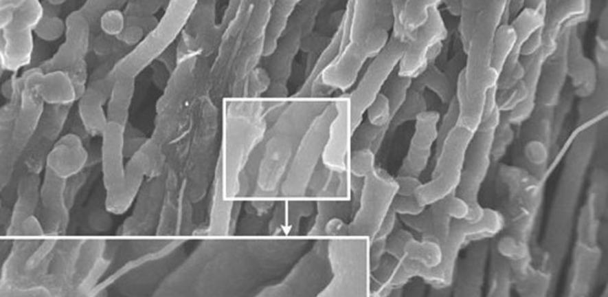
Nanowires will be a key area of investigation for Nathan in the coming years. These structures have an extraordinary length-to-width ratio, only a few nanometres in diameter, and a much greater capacity in terms of speed. “Uniformly dispersed over large areas, the wires could result in millions of transistors on a single sheet of A4 for example,” says Nathan.
“While it hasn’t been done yet, we will be working on this in an attempt to match the speeds of a Pentium-like chip, scaled to A4. Pentium chips cost 10 dollars per centimetre squared, while a nano thin film transistor could cost as little as 10 cents per centimetre squared, a much cheaper alternative.”
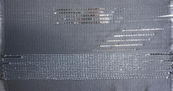
Industries such as biomedicine could also benefit hugely from this interlacing of nano-electronics into materials. “You could foresee a time when you can take the X-ray to the patient rather than vice-versa,” says Nathan. “Patients might lie on a surface woven with electronics, so that data can be broadcast straight from the material. You couldn’t do this with Pentium-like chips because of yield and cost issues.”
“With these non-conventional materials you have a great deal of freedom. We believe this approach to circuitry in substrates will lead to the creation of smart substances, and once you start thinking about the possible applications, it’s hard to stop: surgeon’s gloves with smart skin, walls of a house that store energy and generate large-scale displays, magazines with interactive video in the pages, devices that dissolve the toxins in water, bio-interfaces in mobile phones with diagnostic capabilities, clothing that generates energy – the possibilities are endless!”
This work is licensed under a Creative Commons Licence. If you use this content on your site please link back to this page.


